With the explosive growth in the demand for chip computing power driven by AI and 5G/6G technologies,the underlying foundations of advanced packaging are undergoing critical transformations:the performance bottlenecks of traditional organic material substrates and silicon-based substrates are becoming increasingly apparent.Glass substrate,with its excellent characteristics of low dielectric loss,high level up degree,is becoming an important direction of the next generation of packaging.
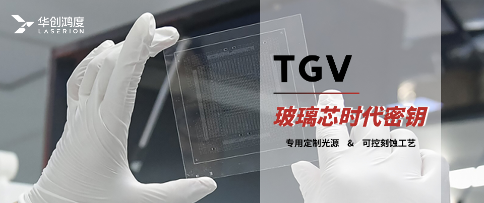
The core technology of glass substrate packaging isTGV(Through Glass Via),i.e.vertical electrical interconnection through a glass substrate.It can significantly improve the efficiency of high-frequency signal transmission,The reduction of thermal stress in packaging process has shown great potential in RF chips,high-end MEMS sensors and high-density system integration,triggering a research and development and layout boom in the global industry.
The global industrial chain has responded quickly to this wave of material transformation.Foreign to Corning, Xinyagao,Schott and other representatives of giants with ultra-thin glass,low melting point glass and other ace products leading the high-end market;Domestic to rainbow,Kaisheng and other companies are also accelerating technology research and development and market layout.According to Global Growth Insights forecast analysis:The TGV substrate market size is expected to be about $129 million in 2024,and is expected to grow to $1.83 billion by 2033,with a CAGR of 34.2% from 2025 to 2033.
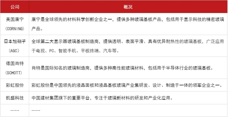
△Famous Supplier of Glass Gubstrates
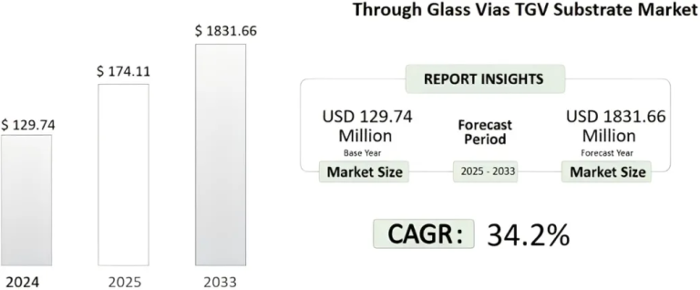
△Global Growth Insights Predictive Analysis
The explosive growth of industry and the diversified development of material systems promote each other,and at the same time force the through-hole processing technology of TGV to evolve towards a higher consistency standard.Advanced processing capability is becoming the core element of industrial chain competitiveness.
TGV is based on high-quality borosilicate glass or quartz glass,through seed layer sputtering, electroplating filling,flattening and RDL re-wiring process to achieve three-dimensional interconnection.The diameter of the microvia is usually 10-100 μm,and the monolithic wafer needs to integrate millions or even tens of millions of metallized vias to meet the electrical connection requirements.In this complex process system,TGV faces three core challenges:high-precision hole making,high-quality metal filling and High density wiring.Among them,high-precision hole forming is the basis of the subsequent process,its quality directly determines the performance and reliability of the packaging structure.
After comprehensive comparison of various hole-making technologies,the laser-induced etching method has comprehensive advantages in machining precision,deep-to-diameter ratio control,hole wall quality and machining flexibility,and is regarded as the most industrialized potential direction by the industry.The Act is divided into two specific steps:① Laser Modification:Selective modification of glass using ultra-fast pulsed laser to form an easy-etching region;② Etching through holes:using chemical etching solution to quickly etch the modified area to form through holes.
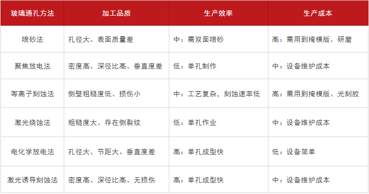
△Graph of the Comparison of Several Perforation Technologies
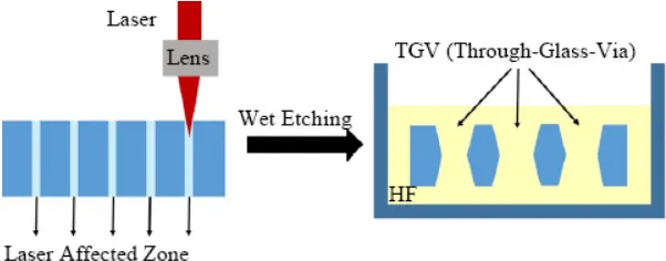
△Laser-induced Carving to Make Pores
The laser-induced etching method combines the advantages of laser and chemical etching:it avoids the problems of micro-cracks and low efficiency caused by laser ablation,and solves the limitation of pure chemical etching in directional processing.By adjusting laser parameters and etching conditions,high precision control of through-hole morphology can be achieved,which lays a solid foundation for subsequent high-quality metal filling and high-density wiring,and strongly supports the large-scale application of TGV in high-frequency signal transmission and high-reliability packaging scenarios.
In the face of the industrialization challenge of TGV technology,Huachuang Hongdu has launched the”dedicated laser source+self-controlled etching process”complete solution,helping the industry to break through the bottleneck of advanced packaging technology.
On the laser light source side,The custom-made TGV superfast laser developed by the company has femtosecond pulse width, superior beam quality(M²<1.2)and high pulse stability(<2%),which ensures the precision of machining from the source and minimizes the thermal effect.During the etching process In this regard, Huachuang Hongdu has mastered the full process of independent and controllable technology, and can flexibly adjust the special etching reagent according to the glass composition.Through precise control of parameters such as concentration,temperature and treatment time,to achieve high depth-to-diameter ratio(>20:1),low roughness(controlled to below 1nm)high-quality channel preparation.
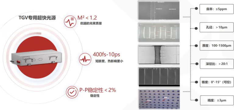
△Huachuang Hongdu TGV Special Light Source Intention
△ Scanning Electron Microscopy of the Inner Wall of the Pore After Etching
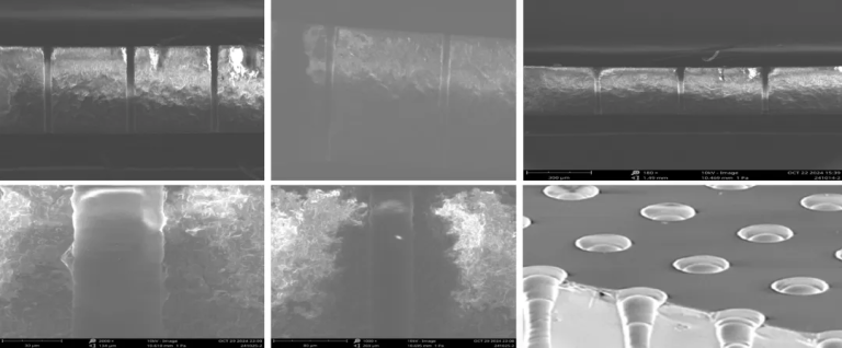
The program has the advantages of fast hole forming speed,no leakage holes,uniform hole diameter,small side wall roughness,no edge collapse and no microcracks.It supports the flexible machining of through holes or blind holes,the hole shape and taper can be controlled,and meets the needs of industrial-scale manufacturing.The high depth-to-diameter ratio structure helps to realize more interconnection channels in a limited space to enhance the integration density and performance of the chip.
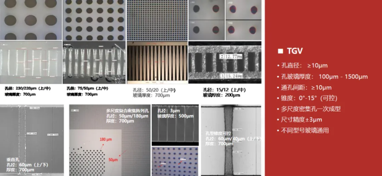
△Cross Section and Morphology of TGV Sample
At present,the programme has successfully produced TGV samples with excellent key indicators,demonstrating a strong production capability to translate the theoretical advantages of glass substrates into product effectiveness,providing a practical path for advanced packaging towards greater performance and reliability.
The industrialization process of TGV technology,as the key path of advanced packaging,is highly dependent on the maturity of perforation technology.The laser-induced etching process,which is the focus of Huachuang Hongdu,is the core link to promote the glass substrate from”material innovation”to”large-scale application.”
Based on the forward-looking insights into the potential of ultrafast lasers in the advanced packaging field, the company will continue to cultivate the key aspects of TGV technology in high-performance computing packaging, continuously promote the technological iteration, help customers to seize the opportunity in the industrial wave, and jointly push the industry to a new height.