With the rise of chip interconnection, the circuit structure has become more complex, and the threat of hidden defects to the good rate has increased significantly. How to detect short circuits, broken circuits and other problems and accurately dispose of them without destroying the circuit is the first task in the field of semiconductor integrated circuits to improve device performance and good efficiency.
Driven by this demand, laser technology has entered the public eye with its characteristics, opening new paths for circuit detection and repair.
When conducting electrical testing, it is usually necessary to remove the insulation layer on the surface of the device or the electrodes of the voltage-sensitive device to perform testing on the underlying electrodes and the circuit structure. At present, the mainstream still uses traditional methods such as mechanical window opening and chemical etching, and the following pain points have long been present:
Against this background, realizing the full-process closed loop of “lossless peeling insulation layer – accurate detection – high success rate repair” has promoted the deep application of laser technology in the field of precision circuit detection and repair.
Huachuang Hongdu relies on its core light source advantages to customize and develop targeted process solutions to form a complete closed-loop system of ” oxidation layer removal, detection and repair. “
①Laser Stripping – high Accuracy and Lossless Opening of Windows
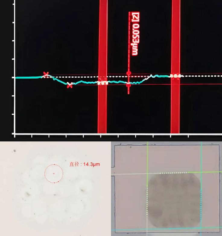
△Microscopic Measurement of Electrode Oxidation Layer Removal by Femtosecond Laser Processing
The objective of the stripping process is to accurately remove the insulation layer or oxidation layer without damaging the underlying circuit, exposing the electrode or circuit to be tested。A femtosecond laser“Precise control of energy , both processing quality and efficiency, no heat accumulation effect”The performance advantage, can be achieved without damage to the electrode under the premise of removing the area of the oxide layer precision ≤ 1 μ m, residual oxide volume ≤ 1%. After the stripping is completed, the electrode function is confirmed by electrical re-inspection, and the fault point is accurately located, and the subsequent laser precision repair of circuit defects is carried out.
②Laser Repair – High Precision Repair of Circuit Defects
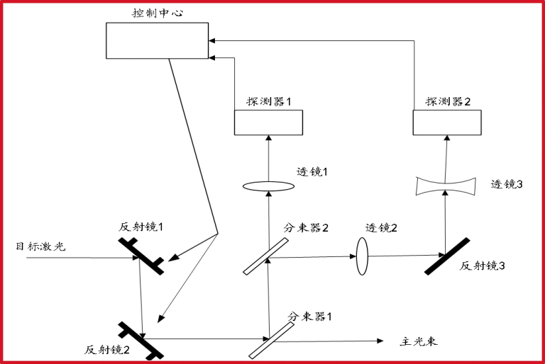
△ High stability precision optical system
A break is a discontinuity (such as a scratch, corrosion, or material defect) in a circuit that is supposed to be connected, causing a signal discontinuity. Using laser-induced localized deposition thin film technology, it can accurately “bridge” the fault and restore the electrical connection.The principle is to use high-energy ultraviolet pulsed laser to bombard the target material, make it instantaneous vaporization and form plasma plume , the material in the feather is deposited and epitaxially grown into a film at the defect site of the substrate induced by the infrared laser heating , which can realize the precision of the film repair area ≤ 1 μm² of high precision and controllable repair.
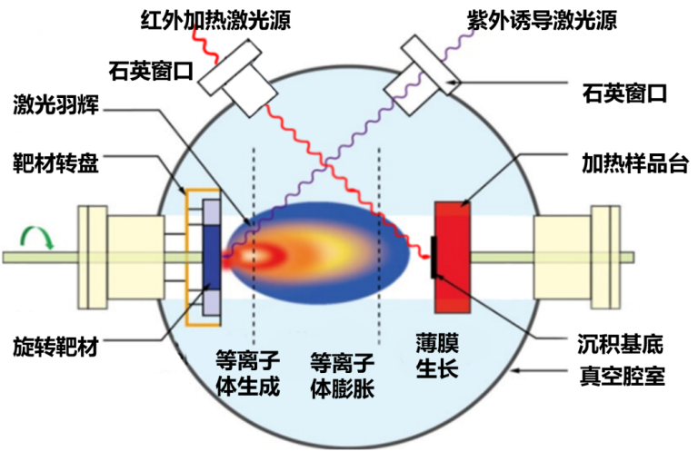
△ Laser-Assisted Vapor Deposition Process: Multi-Physics Coupling-Technology Principle
Short circuits usually caused by metal residue, bridge or dielectric breakdown, manifested as adjacent lines abnormal conduction.With its “high precision” and “cold processing” characteristics, femtosecond laser processing can vaporize to remove excess metal or conductive residue without damaging peripheral circuits.Through active control of the direction of the light source and matching the focal length of the zoomable lens, it is possible to repair the area of short circuit defects with an accuracy of ≤ ± 1 μm².In addition, laser repair has higher flexibility and repair efficiency than in-situ growth film technology without photolithography process.
③Laser fire reduction – high-precision localized heat induced modification
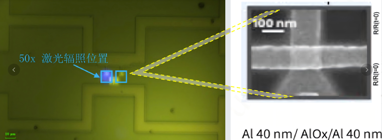
△ Microstructure of Annealed Test Sample
Laser annealing uses local precision heat treatment to reduce surface defects and impurities in the circuit, improve local structure and electrical properties, and precisely correct abnormal resistance values. By precisely regulating specific wavelength laser parameters, the target area is heated to the desired temperature range in a very short time and then cooled quickly.Combined with high stability laser and dual color radiation temperature measurement technology, Can ensure annealing temperature stability ≤ ± 1℃, annealing repair positioning accuracy ≤ ± 1 μm, finally achieve single induction accuracy ± 5 Ω , resistance of the repair area increased by 10 ~ 50 %.
The three key processes and testing links are deeply coupled, forming a closed-loop process of ” peeling – testing – repairing – re-testing , ” and can support a fully automated loading and unloading module , greatly improving yield and efficiency.
The reason why this laser processing scheme can be realized stably lies in the independent control of the core light source – this is precisely Huachuang Hongdu ‘s ability foundation. We focus on high-reliability solid-state laser technology. At present, we have built a complete technology path from core light source RD, mass production to laser application process testing for new scenes and new materials. Welcome enterprises and research institutions to discuss in depth, obtain customized support, and jointly contribute to the steady development of China’s smart manufacturing and China’s “core.”